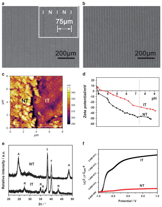
Figure 2.
Construction of the microscale electrostatic field (MEFs). (a, b) Scanning electron microscopy (SEM) images of constructed MEFs with different charged domain intervals ((a) 75 μm interval, (b) 30 μm interval) on the titanium surface. N refers to NT (non-irradiated n-type semiconducting anatase TiO2 zone prepared by hydrothermal synthesis), and I refers to IT (n-type semiconducting rutile TiO2 zone prepared by laser irradiation of the anatase TiO2 zone). The inset is the magnified view of the SEM image. (c) Kelvin probe force microscopy (KPFM) image of the border of the NT (left) and IT zones (right) of the MEF sample with a 30 μm interval showing that the relative potential on the NT zone is ~ 19 mV greater than that on the IT zone. (d) The zeta potential analysis of the MEF sample suggests that the zeta potential around a pH of 7.4 for NT is less than that for IT. (e) X-ray diffraction (XRD) patterns of NT and IT indicate the NT and IT are mainly composed of anatase and rutile, respectively. A, anatase; R, rutile; T, titanium. (f) Mott–Schottky plots for the NT and IT surface indicating they are both n-type semiconductors, and their carrier density (ND) values were 1.82 × 1019 cm −3 and 9.18 × 1020 cm −3, respectively.

