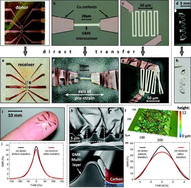
Figure 2.
Direct transfer of two sensor designs (respective panels are separated by the dashed line): a) A GMR microsensor array of different [Py/Cu]30 multilayer elements on the rigid donor substrate. The magnified views in (b,c) show a microsensor stripe and meander, respectively, with the two‐step photolithography for the sensing element and the electrodes. d) A macroscopic serpentine meander consisting of a [Co/Cu]50 GMR multilayer. e–g) Microsensors transferred to the receiving substrate using a uniaxial prestrain of 20%, as indicated in (f). h) The serpentine meander after transfer to the free‐standing PDMS membrane using a biaxial prestrain of 25% × 25%. i) The transferred microsensor array can conform to the soft and curved surface of a fingertip. j) GMR characteristics of a microsensor element before (black) and after (red) the transfer process. k) SEM images of a FIB cut through the transferred GMR film in (h) showing the good adhesion of the wrinkled magnetic nanomembrane to the PDMS support. l) A confocal microscopy image showing the topology of the wrinkled GMR multilayer element in (h). m) GMR characteristics of the serpentine meander before (black) and after (red) the transfer process.

