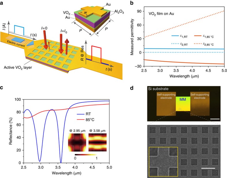
Figure 1. IMT enabled electrically actuated metadevice.
(a) Three-dimensional illustration of the metamaterial device consisting of a sandwich system with a 100 nm-thick patterned-mesh top gold (Au) layer, a 260 nm-thick active VO2 layer and an optically thick (200 nm) Au ground plane. A 50 nm-thick Al2O3 layer is applied in between both gold/VO2 interfaces for optimized device performance. Unit cell of the metamaterial absorber is depicted in the inset where P=1550, nm and w=600 nm. The top patterned gold layer is connected to an external circuit, which simultaneously supports optical resonances and electrical functionality for Joule heating. The reflection of incident light at normal incidence would be immediately tuned as a function of the electrical current flowing through the layer, which triggers the IMT in the active VO2 layer. (b) Measured permittivity of VO2 thin film on top of Au at RT and 85 °C, which clearly indicates the phase transition. (c) Simulated reflectance spectra of the hybrid metamaterial absorber with VO2 layer in the insulator (blue curve) and metallic (red curve) phases. Insets: calculated electric field profiles (|E|2) within the VO2 layer for a unit cell (inset of a) at the wavelengths of 2.95 and 3.58 μm. (d) Photo of the device and scanning electron microscope (SEM) image of the metadevice, with the inset illustrating an enlarged SEM image of a unit cell. The scale bars in the upper and lower panel of d represent 2 mm and 1 μm, respectively.

