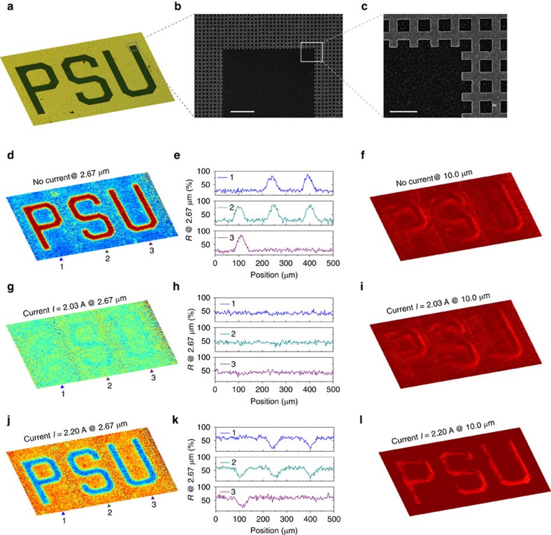
Figure 4. Electrically controlling spatially dependent infrared images.
(a) Microscopic image of the fabricated metamaterials with an area of the top Au layer removed to form the letters ‘PSU'. Geometrical dimensions of imaging: 900 × 500 μm2. (b,c) Scanning electron microscope (SEM) images of a corner of the patterned letter ‘U'. The top gold meshes, which are connected to external circuitry, correspond to the olive area in a, whereas bare VO2 forms the letters in dark green in a,d,g,j, infrared images at a wavelength of 2.67 μm of the metamaterial with various electrical currents applied. Interestingly, as illustrated in g, the letters became invisible in the infrared image at a proper electrical current intensity. (e,h,k) The corresponding reflectance distribution across each of the letters at locations labelled by ‘1', ‘2' and ‘3'. (f,i,l) Infrared images of the device at wavelength of 10.0 μm. No obvious image tuning effect is observed. Scale bars, 10 and 2 μm (b,c).

