Figure 2.

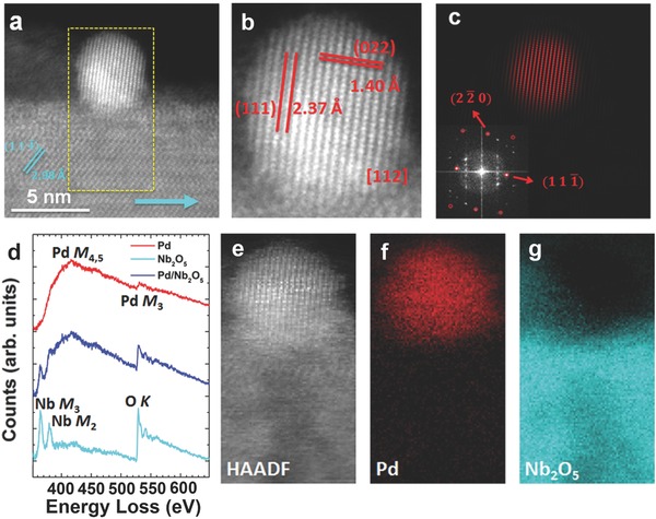
a) HAADF image of a Pd nanocrystal decorated Nb2O5 nanorod. The cyan arrow indicates the [010] growth direction of the nanorod, and the dashed yellow rectangle marks the area where EELS elemental mapping was taken. Scale bar, 5 nm. b) Enlarged image showing nanocrystalline Pd viewed from its [112] direction. The d‐spacing of the (111) and (022) planes was measured. c) Inverse FFT by masking spots only contributed from Pd, as indicated in the inserted figure by the red circles. The inserted figure is the FFT of (a), showing an overlap of contributions from Pd and Nb2O5. d) EEL spectra from the Pd nanocrystal (red), Nb2O5 nanorod (cyan), and interface between the Pd and Nb2O5 (blue). The Pd M4,5‐edge and Pd M3‐edge are visible in the red spectrum; the Nb M3‐edge, Nb M2‐edge and O K‐edge are visible in the cyan spectrum; a superposition of these edges are exhibited in the blue spectrum. e) HAADF image taken while simultaneously collecting the EELS map. f) Fitting coefficient of Pd showing the spatial distribution of the Pd signal. g) Fitting coefficient of Nb2O5 showing the spatial distribution of the Nb2O5 signal.
