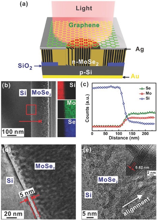
Figure 2.

a) Schematic illustration of the Gr/MoSe2/Si heterojunction photodetector with graphene transparent electrode. b) Cross‐sectional TEM image of the interface of MoSe2 and Si. Insets show the EDS element mappings of Si, Mo, and Se at the red square area. c) The line‐scan EDS analysis along the red line from Si to MoSe2 film in (b). d) HRTEM image of the heterojunction, indicating the existence of an interfacial oxide layer (≈5 nm). e) HRTEM image of the MoSe2 film, verifying the vertically standing layered structure of the film. Inset shows the enlarged HRTEM image. The distance between two layers is ≈0.62 nm, corresponding to the (001) face of MoSe2.
