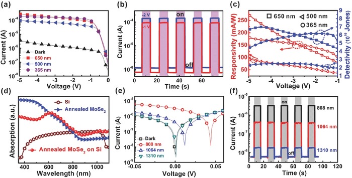
Figure 4.

a) I–V characteristics of the Gr/MoSe2/Si photodetector measured in the dark and under light illumination with varied wavelengths of 365, 500, and 650 nm, respectively. Three‐layer graphene was used as the transparent electrode. The light intensities of the light sources were fixed at 15 mW cm−2. b) Time‐dependent photocurrent excited by pulsed light at 365 nm (15 mW cm−2). Different bias voltages of −1 V and −2 V were applied. c) Plots of responsivity and detectivity of the device at varied light wavelengths as a function of applied reverse bias. d) Absorption spectrum of the MoSe2 film on Si substrate. The absorption spectra of MoSe2 film grown on quartz substrate under the same conditions and bare Si substrate were also plotted for comparison. e) I–V characteristics of the device measured in the dark and under laser illumination with different wavelengths of 808, 1064, and 1310 nm, respectively. The light intensity was maintained at 15 mW cm−2. f) Photoswitching curves of the device in response to pulsed light illumination with various wavelengths at a bias voltage of 0 V.
