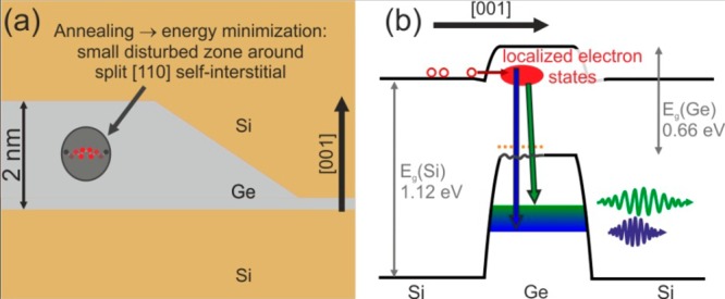
Figure 3.

(a) Recrystallization to a split-[110] self-interstitial with surrounding lattice deformation upon annealing or overgrowth with Si at high sample temperature. (b) Proposed energy level diagram in the [001] growth direction. The full red oval depicts localized Γ-point electron-states at the defect site. The green and blue arrows show GIB-QD PL emissions of longer and shorter wavelengths, and the hole states in the GIB-QD are indicated by the green-blue-shaded area. Parasitic hole states above the VB edge of Ge are indicated by the dotted orange line.
