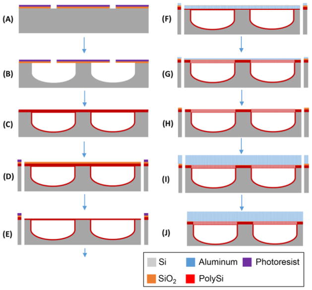
Figure 2.
Illustration of microfabrication process for microdialysis probe. The channel line was patterned on 2 μm thick SiO2 grown Si wafer (A). Semicircular shaped channels with 60 μm wide and 30 μm high were etched by XeF2 (B) and sealed with polysilicon (C). After 1 μm thick SiO2 was deposited, probe shape was patterned and etched by DRIE (D). Sampling area at the tip of the probe was opened and etched by DRIE to be 2 μm thick layer (E). 400 nm Al layer was deposited and anodized electrochemically forming nanoporous AAO membrane (F). Polysilicon layer was etched through AAO membrane by DRIE (G) and 400 nm AAO membrane was removed (H). For physical strength of sampling area, 3 μm AAO membrane was fabricated by the deposition and electrochemical anodization of Al layer (I). Finally, thinned probes were released in hot water after backside etching (J).

