
Figure 7.
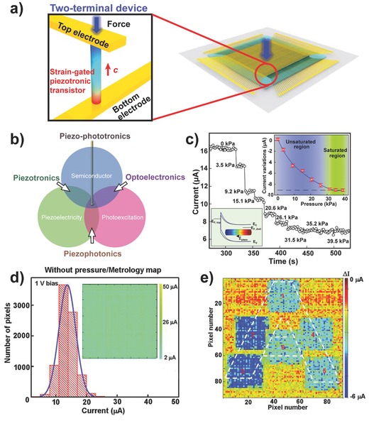
Pressure mapping based on piezotronics. a) Schematic structure of a 3D strain‐gated vertical piezotronic transistor matrix. The color gradient in the enlarged view inset illustrates the piezopotential field induced by the applied force, in which red and blue, respectively, represent positive and negative piezopotentials. b) Origins of piezotronics, piezo‐phototronics, and piezophotonics, which provide the coupling between/among the semiconductor, piezoelectricity, and photoexcitation. c) Current response of a piezotronic transistor to applied pressure. d) Statistical current distribution of the integrated transistor array without applied pressure. e) Current distribution of the array under pressure. Reproduced with permission.[[qv: 15b]] Copyright 2013, American Association for the Advancement of Science.