Figure 5.

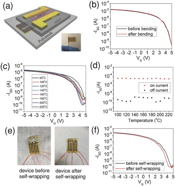
Effects of bending, temperature, and self‐wrapping on SWNT transistor characteristics: a) Schematic diagram of the device structure and bending of the device (inset: image of the bent device around a wire of 0.75 mm radius). b) Transistor characteristics of the device before and after bending at a 0.75 mm bending radius. c) Transistor characteristics of the device after heating to a temperature up to 220 °C with a bending radius of 0.75 mm (measurements were taken at room temperature after heating). d) On and off current of the device at different temperatures. e) Image of a SWNT transistor before and after self‐wrapping process. f) Transfer characteristics of the device before and after self‐wrapping process.
