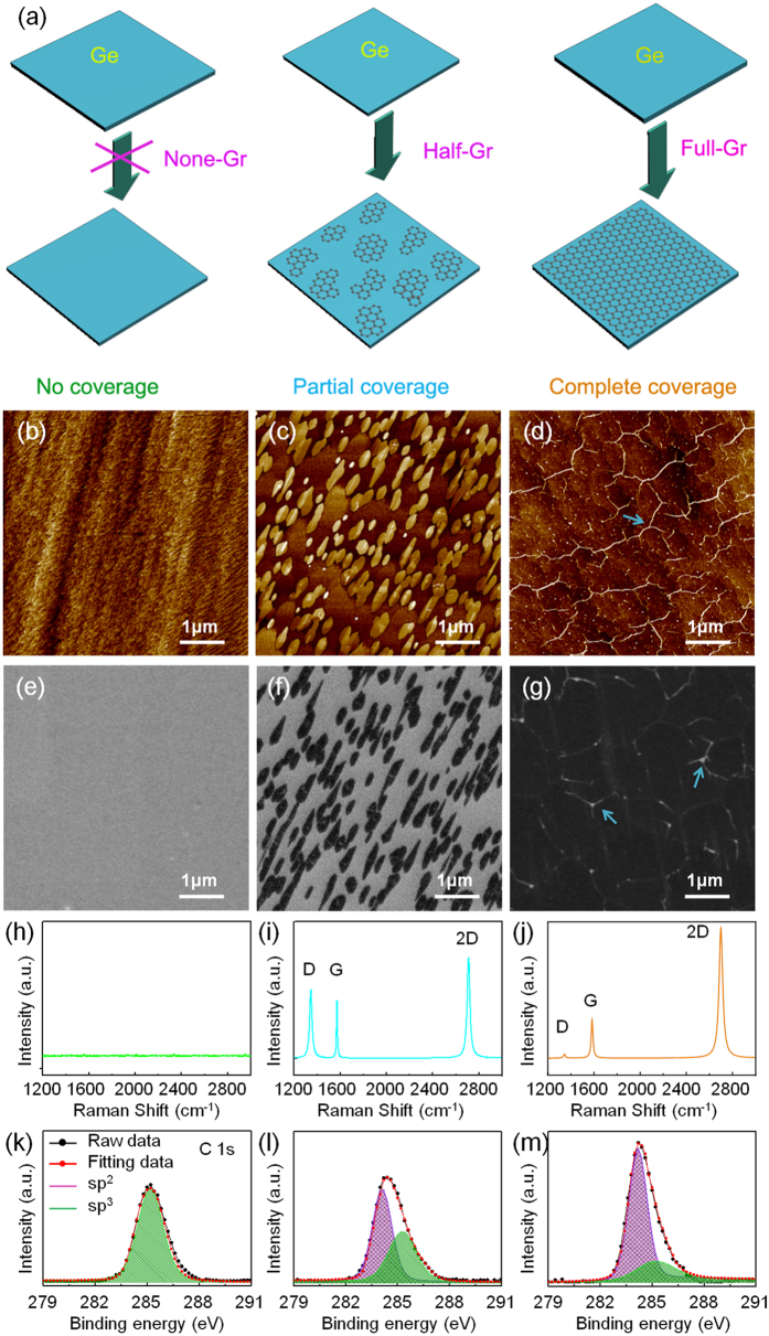
Figure 1.
First panel (a): Schematic fabrication processes corresponding to three typical graphene covered Ge substrates with different coverages, i.e., bare Ge substrate (None-Gr), partially covered Ge substrate (Half-Gr) and fully covered substrate (Full-Gr); second panel: (b–d) AFM morphologies of None-Gr (b), Half-Gr (c) and Full-Gr (d) samples, respectively; third panel: (e–g) SEM morphologies of None-Gr (e), Half-Gr (f) and Full-Gr (g) samples, respectively; fourth panel: (h–j) Raman spectra of None-Gr (h), Half-Gr (i) and Full-Gr (j) samples; bottom panel: (k–m) XPS measurements of None-Gr (k), Half-Gr (l) and Full-Gr (m) samples; the blue arrows in (d) and (g) indicate the wrinkle.

