
Figure 3.
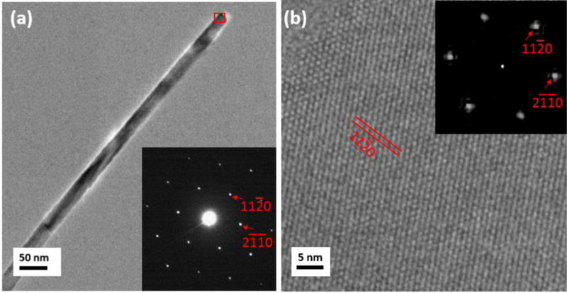
(a) a TEM image of an α-Fe2O3 nanowire before the reduction treatment, the inset is a nanodiffraction pattern taken from the region indicated by the red box, revealing the [0001] zone axis of α-Fe2O3; (b) a representative HRTEM image obtained from the α-Fe2O3 nanowire in the area marked by the red box shown in (a), revealing the perfect lattice structure in the un-reduced nanowires. The inset is a diffractogram (fast Fourier transform) of the HRTEM image. The surface plane of the nanowire is .