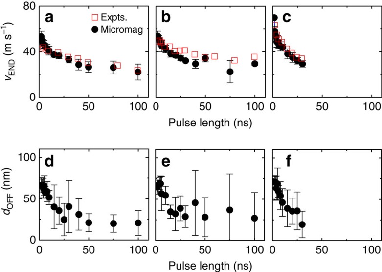
Figure 5. Comparison of experiments and micromagnetic simulations.
(a–c) Quasi-static domain wall (DW) velocity vEND (red squares) measured as a function of pulse length for three different pulse amplitudes: (a) 16 V (J∼0.5 × 10⁸ A cm−2) (b) 20 V (J∼0.6 × 10⁸ A cm−2) and (c) 25 V (J∼0.8 × 10⁸ A cm−2). All results are from film set B, wire width is ∼5 μm and the W layer thickness d is ∼3 nm. The black circles show calculated vEND using micromagnetic simulations with two dimensional pinning. The average velocity is obtained from 5 different randomly generated grain patterns. (d–f) Average distance DWs travel after the current pulse is turned off (dOFF) calculated using micromagnetic simulations. The error bars indicate distribution due to different grain patterns used in the simulations.

