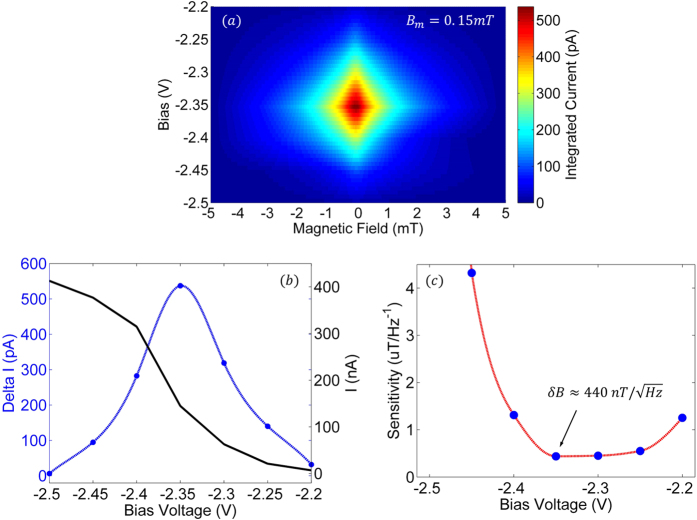
Figure 3.
Panel (a) illustrates the change in current ΔI as a function of applied magnetic field and junction bias. The other two plots illustrate (b) the change in current ΔI at B = 0 mT and DC current I0 and (c) sensitivity δB as a function of applied junction bias. Note that for this particular SiC device, a forward bias of 2.35 V yielded the optimum sensitivity of  .
.

