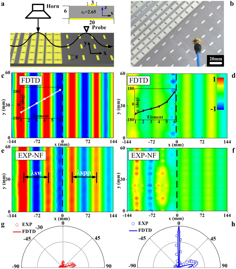
Figure 5. Near-field characterizations on the tunable metasurface: Dynamical functionality switching.
(a) Schematics of the PW-SW conversion setup. Inset shows a unit cell of the mushroom structure, consisting of a metal bar (sized 3 mm × 8 mm) coupled with a continuous metal plate through a 6 mm – thick dielectric spacer (εr = 2.65). (b) Picture of the fabricated sample and the near-field probe. (c,d) FDTD simulated and (e,f) measured Re(Ez) distributions under (c,e) the voltage combination corresponding to frequency 4.1 GHz as shown in Fig. 3(c) and (d,f) Vi = 30 V for all elements. Insets in (c) and (d) depict the phase profiles under the specified external voltages. All fields in (c–f) share the same color bar shown in (d). FDTD simulated and measured far-field scattering patterns of the metasurface at 4.1 GHz under (g) the voltage combination corresponding to frequency 4.1 GHz and (h) Vi = 30 V for all elements.

