
Fig 1.
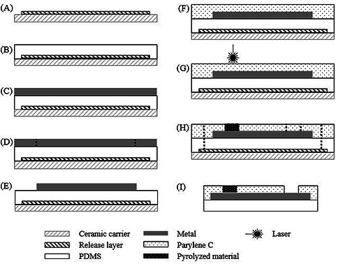
Cross-section schematic of the array process fabrication: A) lamination of the release layer; B) spin coat PDMS; C) lamination of the metal; D) laser structuring of the metal; E) removal of metal excess; F) parylene-C deposition; G) laser pyrolysis; H) contact opening and cut of the electrode borders; I) electrode peel off.