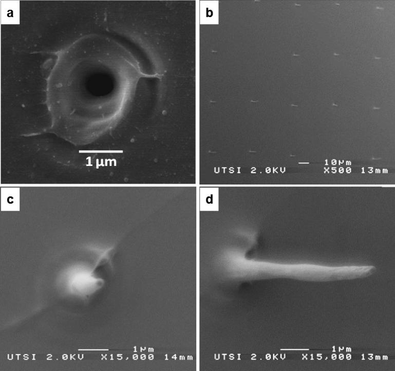
Figure 2. Process characterization.
a) SEM image of a femtosecond laser machined pore on the surface of a fused silica wafer. The pore was opened using a single 3.2 μJ, 790 ηm, 160 femtosecond laser pulse; b) SEM image of a PVA replica (Pt coated, 45° stage tilt). c) A single PVA nanoneedle with a final length of 10 μm. d) same PVA nanoneedle at 30° stage tilt.

