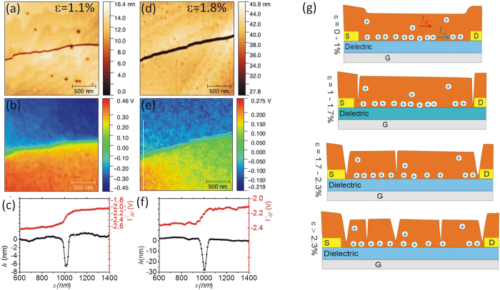
Figure 6. Crack formation in strained microcrystal as observed in AFM experiments on biased transistors and model for OTFT strain response.
(a,d) AFM surface topography; (b,e) SKPM surface potential and (c,f) profiles of height and surface potential across the crack at the two different investigated strain values; (g) Model explaining the OTFT response to tensile strain.

