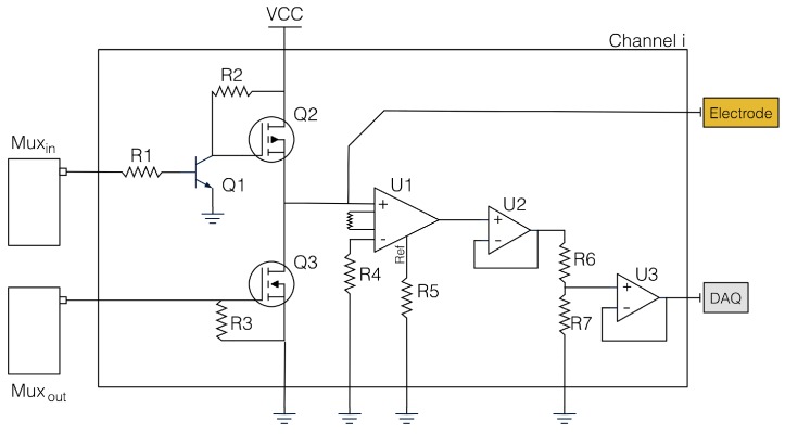
Figure 2.
Schematic overview of the driving and readout electronics. The image depicts the configuration for a generic channel and its components. By using this configuration, a single channel can be set as: (i) current source; (ii) current sink (ground electrode); or (iii) used to measure the electric potentials with respect to an external common ground. The process is controlled by the two independent de-multiplexers connected at each channel. DAQ: data acquisition board. In the figure, Q1 is the NPN transistor, Q2 and Q3 respectively the P-MOSFET and N-MOSTEF, U1 is the INA118, U2 is the OPA827, and U3 is the TLV2371.

