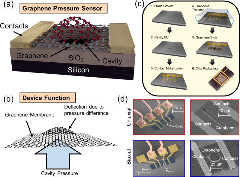
Figure 1.
(a) Schematic of the pressure sensor used in this work. The red area represents the active area of the device. (b) Representation of membrane functionality in a graphene pressure sensor. As the pressure outside the cavity varies, it causes a deflection and straining of the graphene membrane, thereby changing its electronic properties. (c) Fabrication process flow starting with SiO2 growth on a silicon substrate followed by RIE cavity etching. Metal contacts are then patterned followed by the transfer of graphene. The graphene is patterned using a mask in combination with O2 plasma etching. Finally, devices are wire bonded and placed into a chip package. (d) Color-enhanced SEM of a sensor device with a rectangular graphene membrane resulting in uniaxial membrane strain (upper image) and SEM of a sensor device with a circular graphene membrane resulting in biaxial membrane strain (lower image). In the SEMs, the graphene is shaded in blue, the cavity in green, the electrodes and contact pads in yellow, and the bond wires in orange. To the right of each color-enhanced SEM is an SEM showing a close-up of the cavity region for the corresponding devices.

