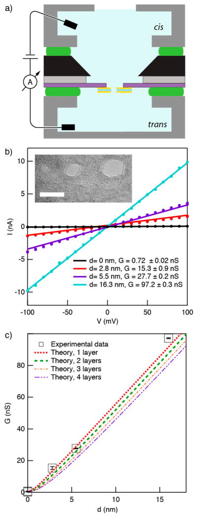
Figure 3.
Ion transport measurements through nanopores in MoS2 membrane devices. (a) Scheme of setup (see text). (b) Current–voltage curves of several nanopores (0.40 M KCl, pH 8, T = 21 °C, pore diameter d and conductance G indicated in legend). Inset shows TEM image of several pores drilled adjacent to each other (scale bar = 5 nm). (c) Comparison of our experimental G and d values with theoretical curves computed for 1–4 MoS2 layers using eq 1.

