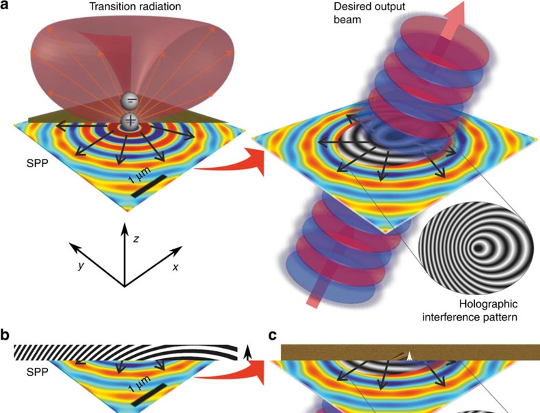
Figure 1. Holographic free-electron light source design.
(a) The electromagnetic excitation resulting from normally incident free-electron impact on a metal surface is computationally replicated by an electric dipole located in close proximity to the surface. The holographic mask required to couple this excitation to a desired output beam is obtained via the interference of the dipole-generated near-field and the required output field, as schematically illustrated for a collimated plane wave at an oblique angle to the surface-normal. (b) Binary version of the as-generated greyscale interference pattern required to produce, from the impact of 30 keV electrons on a gold surface, an output beam at a wavelength of 800 nm directed at 30° to the surface-normal. (c) False colour scanning electron microscope image of the pattern from panel (b) fabricated on an optically thick (140 nm) gold film (scale bar, 10 μm).

