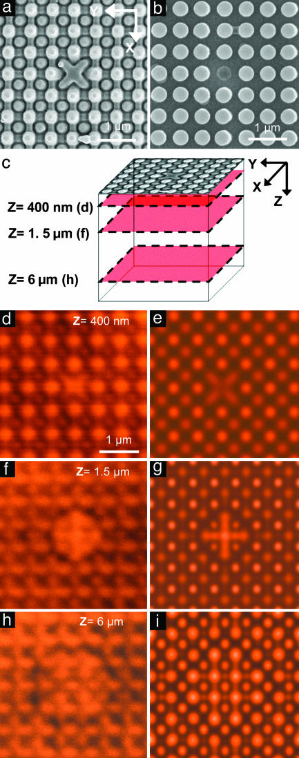
Fig. 3.
SEM, schematic, confocal micrographs (Leica SP2), and optical modeling illustrating the geometry of an aperiodic structure made with a specially designed conformable phase mask. (a) SEM image of the surface of a 3D nanostructure formed by using mask 1 with an isolated missing post. (b) Topview SEM image of this mask. (c) 3D perspective view of x–y cross-sectional plane. (d–i) Confocal image of x–y plane and modeling at z depths of 400 nm (d and e), 1.5 μm(f and g), and 6 μm(h and i).

