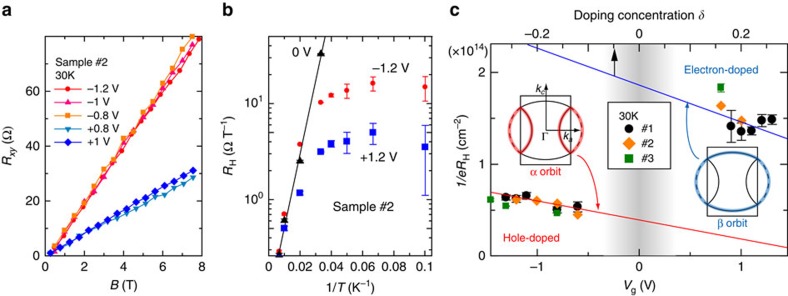
Figure 3. Hall effect.
(a) Hall resistance versus magnetic field at 30 K. (b) Temperature dependence of RH at Vg=−1.2, 0 and +1.2 V. The solid line represents the fit 8.78 × 10⁻² × exp (Ea/kBT) ΩT−1 with an activation energy Ea/kB=176 K to the data of the undoped bulk crystal. The error bars were calculated from the s.d. of the Hall resistance versus magnetic field plots. Note that the data below 25 K contain further errors owing to the non-ohmic behaviour (Supplementary Note 6). (c) Gate voltage dependence of 1/eRH at 30 K. Data from three different samples are shown. The solid lines denote the 1/eRH estimated from the volume bounded by the non-interacting FS (blue) and by the lens-like closed portion of the FS (red). Namely, the blue and red solid lines represent densities of the total carriers and the partial carriers enclosed by the lens-like closed portion, respectively. Here, the electron doping concentration δ is related to the non-interacting hole density n (=1−δ) which is evaluated for the anisotropic Hubbard model with U=0. On the basis of the FET and EDLT measurements, the top horizontal axis is set in that δ=0.2 corresponds to Vg=1 V (see Supplementary Note 1).

