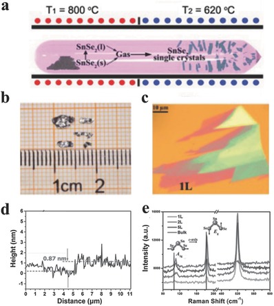
Figure 2.

a) The schematic illustration of the growth of SnSe2 single crystals using the vapor transport deposition (VTD) technique. b) The optical image of SnSe2 single crystals with the size of several millimeters. c) Optical image of SnSe2 flake placed on the surface of a silicon wafer capped by 285 nm thick silicon dioxide. d) The thickness of monolayer SnSe2. e) Normalized Raman spectra of SnSe2 from monolayer to bulk. The intensity of Si peak is set as constant. (a–e) Reproduced with permission.120
