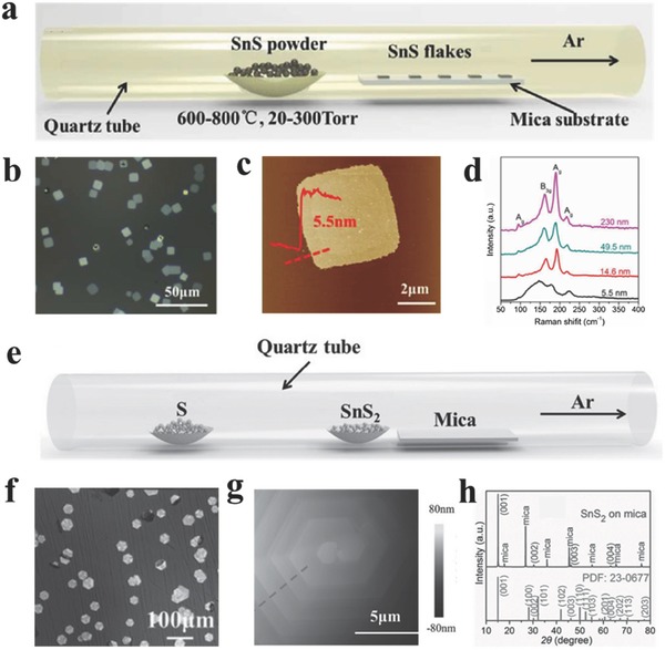
Figure 4.

a) Schematic illustration for PVD growth of 2D SnS flakes. b) Optical image of the 2D SnS flakes. c) AFM image and height information of one 2D SnS flake. d) Raman spectra of the SnS flakes with different thickness. (a–d) Reproduced with permission.79 2016, The Royal Society of Chemistry. e) Schematic illustration for synthesizing 2D SnS2 crystals. f) Optical image of large scale 2D SnS2 crystals. g) AFM image of the center region of a thick crystal showing hexagonal spiral fringes. h) XRD pattern of the SnS2 sample. (e–h) Reproduced with permission.149
