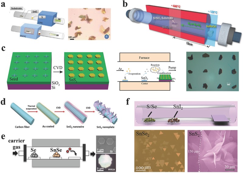
Figure 5.

a) Illustration of the growth process and optical image of the as‐prepared SnS2 flakes. Reproduced with permission.186 2016, The Royal Society of Chemistry. b) The vapor transport set‐up for polymorphic growth of the SnS2 and SnS crystals. Reproduced with permission.130 2015, American Chemical Society. c) Schematic diagrams of patterning seed arrays and the CVD experimental setup, and optical image of the as‐synthesized SnS2 crystal arrays. Reproduced with permission.75 2015, American Chemical Society. d) Schematic diagram of experimental setup. Reproduced with permission.142 2015, The Royal Society of Chemistry. e) Schematic illustration of the synthetic setup, SEM, and optical images of the as‐synthesized SnSe2 nanoplates. Reproduced with permission.188 2013, American Chemical Society. f) Schematic diagram of the CVD synthetic process, optical image of large‐scale SnSe2 nanoflakes (Reproduced with permission.76) and SEM image of large‐size SnS2 nanosheets. Reproduced with permission.118
