Figure 6.

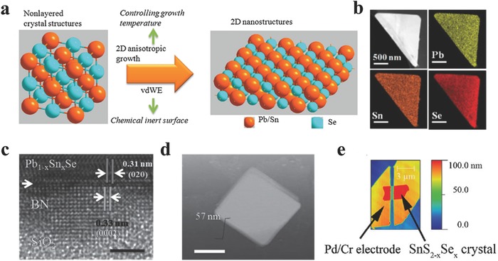
a) Schematic illustrations of van der Waals epitaxial ultrathin 2D Pb1–xSnxSe nanoplates with a cubic crystal structure tailoring into ultrathin 2D nanostructures at certain growth temperature. b) TEM‐EDX mapping of triangle Pb1–xSnxSe nanoplate. c) High‐resolution TEM of few‐layer BN/Pb1–xSnxSe nanoplate heterostructure which denotes a clear interface between BN and Pb1–xSnxSe. The red arrow shows the interface. The lattice mismatch between (020) surface of Pb1–xSnxSe and (0002) surface of BN reaches 6.1%. Scale bar = 3 nm. d) AFM image of a typical Pb1–xSnxSe nanoplate. Scale bar = 2 μm. e) An AFM image of a SnS2–xSex device with x = 0.4. (a,b) Reproduced with permission.104 2015, American Chemical Society.(c,d) Reproduced with permission.107 (e) Reproduced with permission.74 2013, American Institute of Physics.
