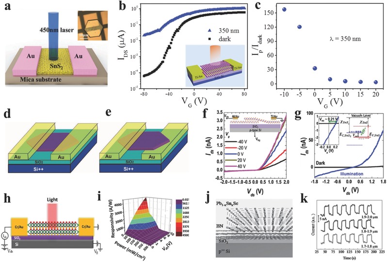
Figure 9.

a) Schematic view of a SnS2 photodetector with 450 nm laser for illumination. Inset shows the optical image of a device. Reproduced with permission.149 b) Transfer curves at light illumination. Inset: schematic diagram of the phototransistor. c) Photoresponse ratio as a function of V g. (b,c) Reproduced with permission.118 d,e) Schematic diagrams of two kinds of single micrometer sized GeSe based photodetector with top‐contact and bottom‐up‐contact. Reproduced with permission.94 f) Gate tunable output characteristics of SnS2/SnS vertical heterostructures, inset: device schematic. g) Dark I–V curve and I ph–V curve under 3.06 eV light illumination with a power of 3.2 μW. Left inset: photovoltaic I–V curves, showing the open‐circuit voltage of 0.21 V. Right inset: corresponding band diagram of the heterojunctions. f,g) Reproduced with permission.130 2015, American Chemical Society. h,i) Schematic of the SnS2–xSex based photodetectors, and 3D view of photoresponsivity mapping of few‐layered SnS2–xSex phototransistor. Reproduced with permission.197 2016, American Chemical Society. j,k) Schematic diagram for epitaxial growth of Pb1–xSnxSe nanoplates on few‐layer BN, and mid‐infrared detection of Pb1–xSnxSe nanoplates at 1.7–2.0 μm. Reproduced with permission.107
