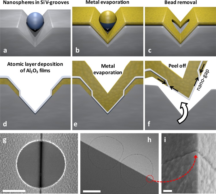
Figure 3.
Atomic layer lithography for wafer-scale production of sub-10 nm gap split-wedge antennas. (a–f) Fabrication process of circular nanogap on wedges via nanosphere lithography, atomic layer lithography, and template stripping. Here micro/nanospheres inside the V-shaped trenches act as masks for metal deposition. (g) After metal evaporation, holes are created in metal films inside the trenches. Alumina is deposited by ALD to define sub-5 nm gaps. A second silver layer is deposited into the wedge. The entire stack is stripped by attaching it to a glass slide with a UV cured adhesive. (h) Two annular nanogaps formed on the wedge. (i) Zoomed in SEM images showing a 5 nm nanogap on silver wedge tip. The scale bars in (g) and (h) are 1 μm. The scale bar in (i) is 100 nm.

