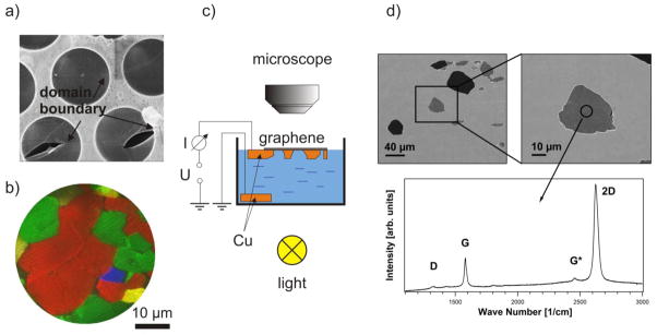
Fig. 7.
a) SEM (4 keV, In Lens detector) image of moderate quality monolayer graphene on an array of 4.5 μm orifices transferred using poly-methyl-methacrylate (PMMA). After the removal of the PMMA protection layer, graphene exhibits a network of cracks along the domain boundaries. The typical domain size is of the order of a micrometer. b) LEEM image of CVD grown graphene on Cu with improved domain size of up to several 10 μm. c) Scheme of local etching of Cu foil with grown monolayer graphene film. d) SEM images of empty (dark) and suspended (grey) holes in the Cu foil. Weak D-band signal together with a pronounced G and 2D band in the displayed Raman spectrum shows that the produced membrane consists of a high quality monolayer graphene [67].

