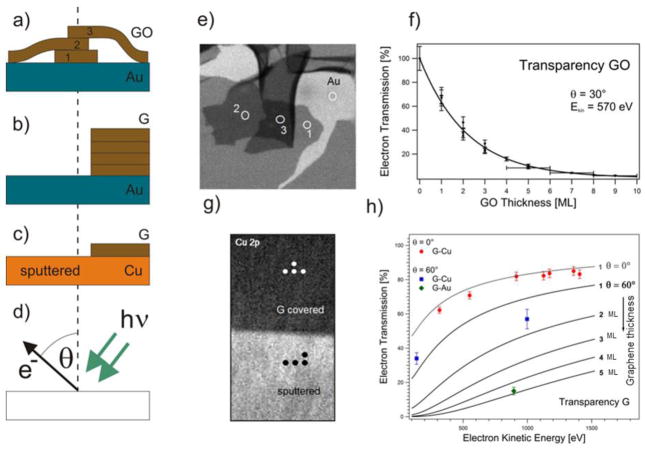
Fig. 8.
a–c: Different sample arrangements for electron attenuation measurements: (a) drop casted GO, (b) wet-transferred multilayer graphene on Au film, (c) locally Ar+ etched monolayer graphene on Cu. d: Geometry of the PE experiment; e: Au 4f image (64 μm × 64 μm) of GO platelets on Au film; f: Evaluated electron transparency of GO platelets for θ = 30° and Ekin = 570 eV. Dots represent independent measurements where the transmission could be determined with an error of about 10%. GO thicker than 5 layers is determined with accuracy of +/− 1 layer; g: Cu 2p image (320 μm× x 640 μm) of the boundary between the graphene covered and sputter cleaned Cu foil. At the indicated spots local XPS spectra were acquired; h: Extracted electron transparency of graphene at θ = 0° and θ = 60° as a function of kinetic electron energy and layer thickness of the graphene film. The data points were derived from monolayer G-Cu and multilayer G-Au/Si. The solid lines (grey: θ = 0° and black: θ = 60°) show the predicted attenuation curves calculated using TPP-2 formula [74,75,33].

