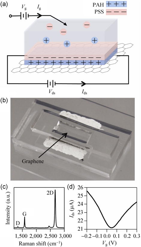
Figure 1.

(a) Schematic illustration of polyelectrolyte multilayers of PAH and PSS deposited on the surface of single layer graphene. (b) Optical image of single layer graphene transistor device. (c) Raman spectrum of single layer graphene transfer-printed from PDMS block to SiO2/Si substrate. (d) Liquid-gated ambipolar field-effect response of graphene device in 100 mM NaCl and Vds = 0.1 V.
