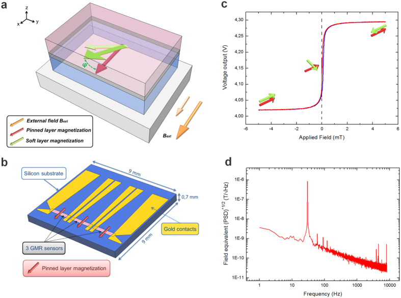
Figure 2. GMR sensors.
(a) Schematic representation of the trilayer structure constituting the spin valve deposited on a silicon substrate (light gray). The pinned layer (light blue) has a fixed magnetization along a specific direction (red arrow). A thin copper layer (dark gray) decouples the pinned layer from the free layer (light pink). An external field applied in the plane of the stack rotates the free layer magnetization, which forms an angle ϕ with the pinned layer, according to the field strength (illustrated with light and dark green arrows according to the external field strength in light and dark orange). The resistance of the stack varies as function of the angle between the free and the pinned layer. (b) GMR sensor configuration. The sensor comprises three segments (light pink) with pinned layer magnetization perpendicular to the segment length (red arrows). Each segment is contacted through two lines of gold/titanium (yellow). (c) Voltage variation of a single segment as function of an in-plane field applied along the pinned layer magnetization. Red (blue) curve is obtained when the field is swept from large negative (positive) values to large positive (negative) values. (d) Field equivalent noise (square root of the voltage power spectrum density (PSD) divided by the sensitivity), of the segments in a magnetically shielded room. The calibration from V/ to T/
to T/ is made by using a calibrated signal at 30 Hz.

