Figure 2.
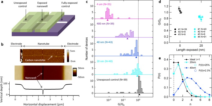
Effect of nanowell-confined chemistry on carbon nanotube devices. (a) Mask design showing a nanowell of controlled position and width over the device channel. Positive and negative controls are designed outside the device channel using full exposure and full protection of the nanotube, respectively. (b) Atomic force microscopy image showing a carbon nanotube between metallic electrodes (top) and the same device covered with a protecting mask opened with a 20 nm nanowell (middle), along with the corresponding height profile (bottom). (c) Distribution of conductance change G/G0 after functionalization within nanowells of different widths, compiled on N individual devices from the same nanotube (Ntotal = 196). Arrows indicate the mean conductance change obtained from a log-normal fit of the distribution. (d) Conductance change and error bars (s.d.) obtained using 20 nm nanowell masks (cyan) compared to control devices (black). Each data point is a N-device average from a different nanotube. (e) Modeled probability of getting a number n of functional groups using small nanowells. Circles represent measured points based on data in panel c; others are extrapolated from a Poisson distribution.

