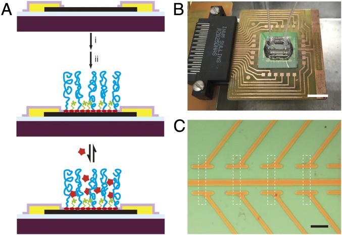
Fig. 1.
Active sensor surface and sensor chip. (A) Illustration of a graphene FET device with comodification of PEG and a small-molecule spacer or PEG and a receptor, for nonspecific and specific detection of the analyte, respectively. Dark purple, silicon wafer; light blue, 600-nm SiO2; black, graphene; yellow, metal contact; light purple, Si3N4 passivation layer; red oval, PYCOOH; green, spacer molecule; blue, PEG chain; red star, analyte. EDC and Sulfo-NHS serve as cross-linkers to couple PYCOOH with PEG and spacer molecules. (B) Optical image of a typical device chip (central green square) mounted on a PCB interface board that is plugged into the input/output interface connected to a computer-controlled data acquisition system. The copper squares surrounding the device chip are connected to the chip by wire bonding. A PDMS microfluidic channel is mounted onto the central graphene region. The inlet/outlet of solution was controlled with a syringe pump via tubing. (Scale bar: 1 cm.) (C) Bright-field microscopy image of two types of graphene channels with dimensions of 5 × 5 and 5 × 10 μm, sharing the common source (S) with individually addressable drain (D) contacts. The white dashed rectangle highlights one graphene FET. (Scale bar: 20 μm.)

