Figure 2.

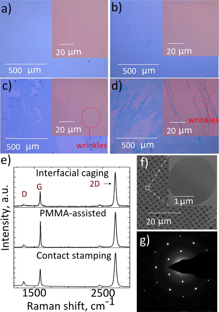
Biphasic transfer contest: comparison with conventional transfer methodologies (PMMA, contact stamping, hexane–water interface). (a) Optical micrograph of graphene transferred using interfacial caging with solidified cyclohexane. (b) Optical micrograph of graphene transferred using the PMMA-assisted method. (c) Optical micrograph of graphene transferred using contact stamping. (d) Optical micrograph of graphene transferred using hexane-assisted method.14 (e) Raman spectra of graphene transferred onto silicon wafers using interfacial caging, PMMA-assisted and contact stamping. (f) Scanning electron micrograph of graphene transferred to quantifoil electron microscopy grids using the interfacial caging. Inset: zoomed-in view of graphene free-standing on top of a hole on the grid—no contamination, cracks, and foldings are visible. (g) Diffraction pattern of graphene transferred with cyclohexane. TEM was carried out with a 300 kV electron beam focused to a 100 nm probe size at low dose.
