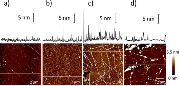
Figure 3.

AFM images and height profiles of graphene samples transferred to silicon wafer using interfacial caging and other conventional transfer methods. (a) Interfacial caging method. (b) PMMA-assisted method. (c) Contact stamping method. (d) Hexane-assisted transfer method.14 The top panel in each image shows the height profile along the line (in white) highlighted in the main image.
