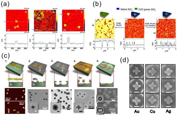
Figure 7.
(a) DNA origami-modulated etching of SiO2 by HF vapor [102]; (b) room-temperature CVD process for SiO2 growth using DNA origami as a mask [104]; (c) fabrication steps to produce high-resolution metallic shapes on the Si surface using DNA origami stencils [105]; (d) similar cross-shaped structures fabricated from different metals via the same origami mask [105]. (a) is reproduced with permission from [102]. Copyright American Chemical Society, 2011; (b) is reproduced with permission from [104]. Copyright American Chemical Society, 2013; (c,d) are reproduced with permission from [105]. Copyright Royal Society of Chemistry, 2015.

