
Fig. 3. The fabrication and characterization of the TPP@PVDF-HFP microfibers.
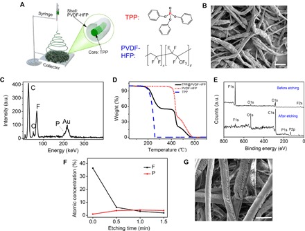
(A) Schematic illustration for the fabrication of the microfibers by electrospinning. (B) SEM image. Scale bar, 5 μm. (C) EDX and (D) TGA measurements of the as-spun fibers. A thin conducting layer of gold was coated onto the fibers for SEM observations. The Au peak in EDX was attributed to the gold layer on the sample. a.u., arbitrary units. (E) The XPS data of the fiber before and after etching (0.5 min). (F) AES sputter depth profiling of the fiber with different etching times. (G) SEM image of the TPP@PVDF-HFP microfibers after etching clearly shows their core-shell structure. Scale bar, 5 μm.