
Figure 16.
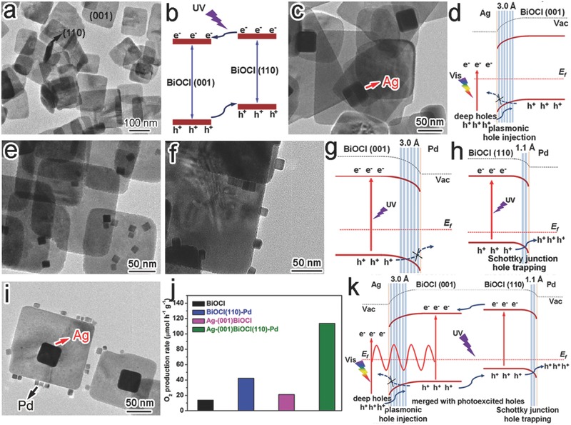
a) TEM image of BiOCl nanoplates. b) Schematic illustration showing the facet‐dependent charge migration in BiOCl. c) TEM image of Ag‐{001}BiOCl. d) Schematic illustration for energy band alignment and hole carrier migration at Ag{100}‐BiOCl{001} interface. e,f) TEM images of (e) BiOCl{001}‐Pd and (f) BiOCl{110}‐Pd. g,h) Schematic illustration for energy band alignment and hole carrier migration at (g) BiOCl{001}‐Pd{100} interface and (h) BiOCl{110}‐Pd{100} interface. i) TEM image of Ag‐{001}BiOCl{110}‐Pd hybrid structure. j) Photocatalytic O2 evolution from water by BiOCl‐based materials under full‐spectrum irradiation. k) Schematic illustrating the band alignment and charge flow at two metal‐semiconductor interfaces in Ag‐{001}BiOCl{110}‐Pd under full‐spectrum irradiation. Reproduced with permission.22