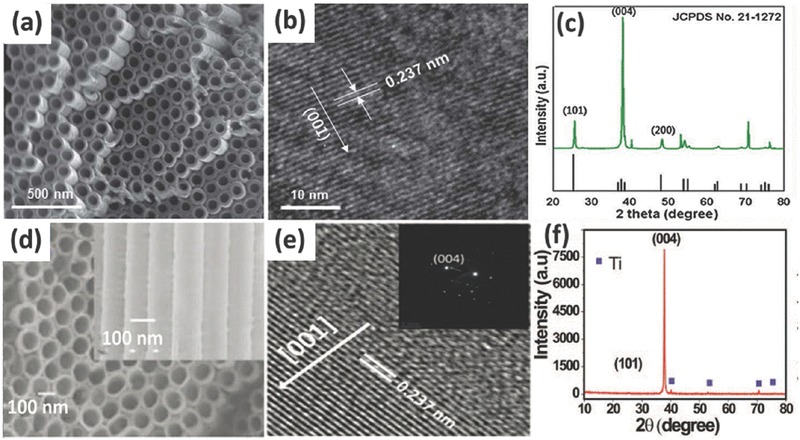
Figure 12.

SEM (a) and TEM (b) images of a TiO2 nanotube array. XRD patterns of TiO2 nanotubes after annealing (c). SEM image (d), high resolution TEM image (e) and XRD image (f) of single crystal like Zn‐incorporated TiO2 nanotubes representatively. (a–c) Reproduced with permission.183 Copyright 2012, Royal Society of Chemistry. (d–f) Reproduced with permission.184 Copyright 2015, Royal Society of Chemistry.
