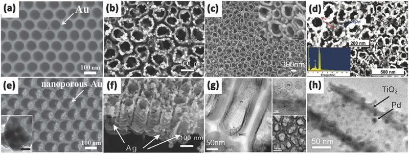
Figure 13.

TiO2 nanotubes after 10 nm Au sputtering (a) and porous Au nanoparticle after dealloying in HNO3 (e). Top view (b) and cross‐sectional (f) SEM images of TiO2 nanotube arrays obtained under pulse current deposition. SEM (c) and TEM (g) images of Pt sputtered on TiO2 nanotube arrays. SEM (inset shows the EDX spectrum of the Pd/TiO2 surface) (d) and TEM (h) image of Pd nanoparticle‐functionalized TiO2 nanotube.(a,e) Reproduced with permission.187 (b,f) Reproduced with permission.198 Copyright 2010, Elsevier. (c,g) Reproduced with permission.199 Copyright 2008, The Electrochemical Society.(d,h) Reproduced with permission.200 Copyright 2008, American Chemical Society.
