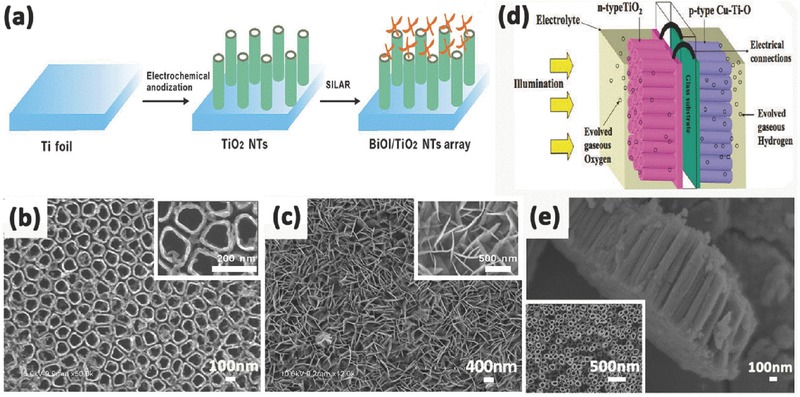
Figure 16.

Schematic illustration for fabricating crossed BiOI nanoflakes/TiO2 nanotubes arrayed structure (a). SEM image of the self‐organized TiO2 nanotubes (b) and 3D interlaced network of BiOI layer on TiO2 nanotubes (c). Illustration of photoelectrochemical diode for water splitting comprised of n‐type TiO2 and p‐type Cu–Ti–O nanotube array films, with their substrates connected through an ohmic contact (d), lateral and top view FESEM images of Cu–Ti–O nanotube array (e). (a–c) Reproduced with permission.213 Copyright 2014, Nature Publishing Group. (d,e) Reproduced with permission.215 Copyright 2008, American Chemical Society.
