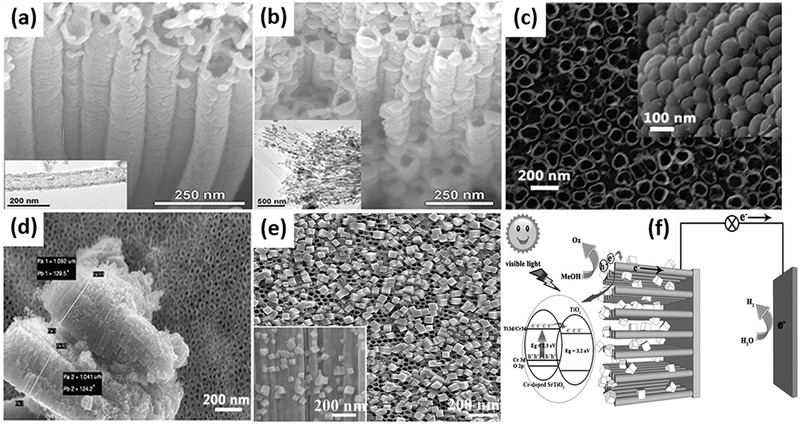
Figure 17.

SEM and TEM (insets) images of (a) TiO2 nanotube array after annealing at 450 °C and (b) TiO2–SrTiO3 hybrid nanostructures obtained after 1 h hydrothermal treatment. Top‐view and bottom‐view (inset) images of Sr‐doped TiO2 nanotubes (c) and its corresponding cross‐sectional views in 0.04 M dopant concentration at pH = 3 (d). SEM images (e) and schematic illustration (f) of charge separation and transport of heterostructured Cr‐doped SrTiO3 nanocube/TiO2 nanotube array heterostructures. (a,b) Reproduced with permission.220 Copyright 2009, American Chemical Society. (c,d) Reproduced with permission.221 Copyright 2011, American Chemical Society. (e,f) Reproduced with permission.223
