Fig. 9.

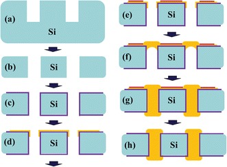
Process flow of proposed sealing bump bottom-up plating approach. a TSV etching. b Thinning. c Oxide insulation. d Seed layer deposition. e Photoresist patterning. f Bump sealing formation. g TSV and bump plating. h Final etching [20]

Process flow of proposed sealing bump bottom-up plating approach. a TSV etching. b Thinning. c Oxide insulation. d Seed layer deposition. e Photoresist patterning. f Bump sealing formation. g TSV and bump plating. h Final etching [20]