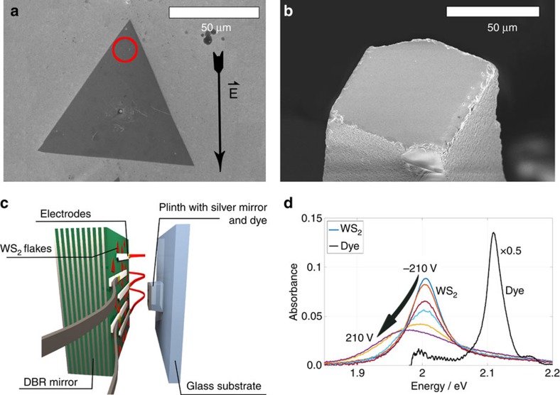
Figure 1. Two-dimensional WS2 between electrodes in an optical microcavity.
(a) SEM-micrograph of a monolayer WS2 flake deposited on SiO2 terminated DBR, forming one side of the optical microcavity. The arrow denotes the direction of the applied electric field and the red circle the area from which the data were obtained. (b) SEM image of the opposing cavity side, a silver mirror on a silica plinth. (c) Sketch of the two mirrors with silver electrodes on the surface of the DBR giving electrical tunability within the cavity. (d) Absorbance of atomically-thin WS2 for various applied voltages obtained from the position marked with a red circle in a (colour) and the organic dye TDBC (black, scaled by factor 0.5).

