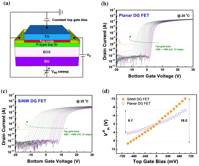
Figure 4.
(a) Schematic of FETs in dual-gate (DG) operation. Transfer curves of (b) planar DG FETs and (c) SiNW DG FETs with constant top gate biases from –600 mV to 600 mV in steps of 60 mV, as indicated by the arrow. The drain bias is 50 mV. (d) Top gate bias versus plot for planar and SiNW DG FETs. for each top gate bias is defined as the bottom-gate voltage corresponding to ID of 1 nA.

