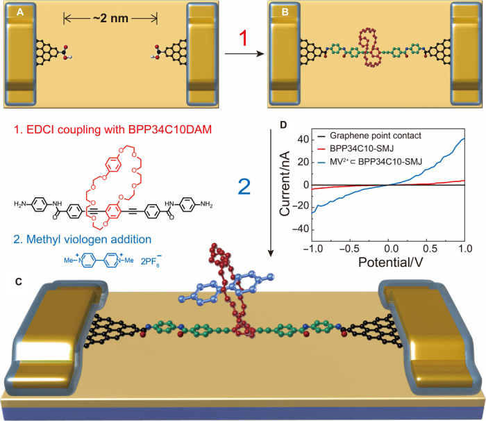
Fig. 1. Fabrication and electrical characterization of SMJ devices.

(A) Schematic representation of graphene point contacts. The carboxylic acid–terminated graphene point contact arrays were formed with ~2-nm gaps during the dash-line lithographic process. (B) Schematic representation of the BPP34C10-SMJ. After treatment with BPP34C10DAM solution in the presence of EDCI coupling reagent, the BPP34C10-SMJ was formed by bridging the conjugated molecular wire across graphene point contacts. (C) Schematic representation of the MV2+⊂BPP34C10-SMJ. The BPP34C10-SMJs were treated with MV to form MV2+⊂BPP34C10-SMJ by immersing BPP34C10-SMJ in an MV·2PF6 Me2SO solution for 12 hours (light brown, SiO2 substrate; blue, silicon substrate and electrode protection layers; gold, gold electrode). (D) Current-voltage (I-V) curves of graphene point contacts (black), BPP34C10-SMJ (red), and MV2+⊂BPP34C10-SMJ (blue) in the solid state. The black curve shows that no current occurs after etching; enhanced current (red curve) indicates a successful single-molecule connection; a further increase in current (blue curve) was observed after the addition of MV·2PF6.
